
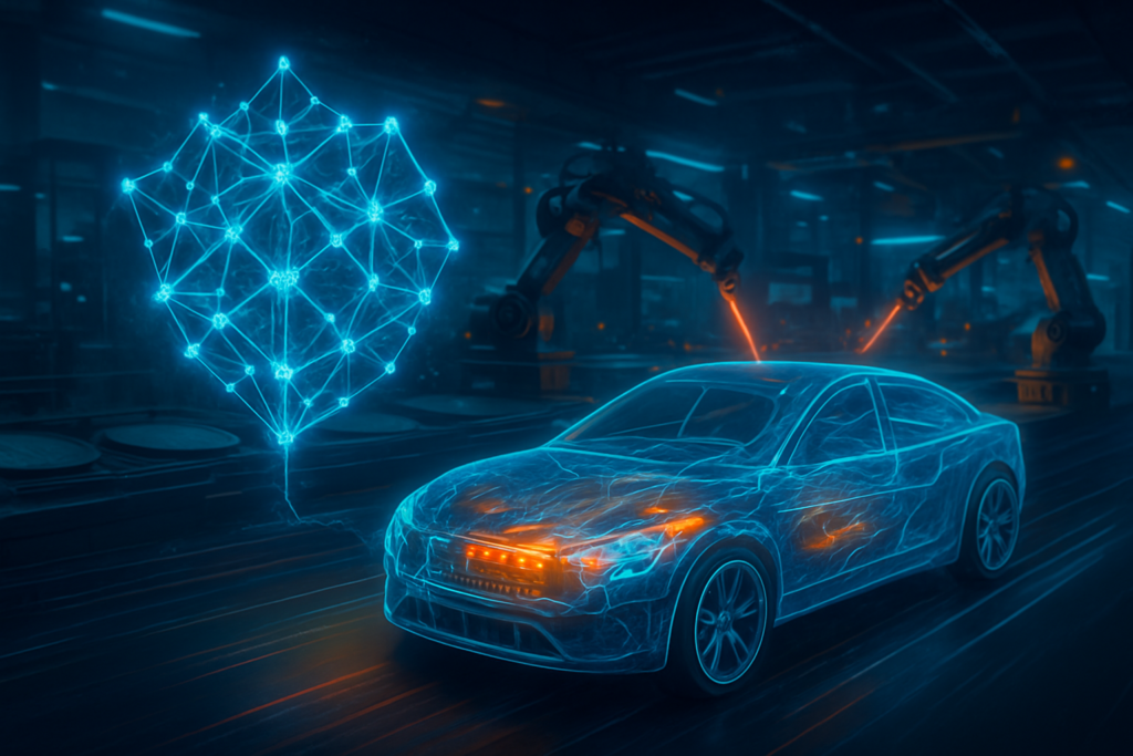
As of early 2026, the global automotive and energy sectors have reached a definitive turning point: the era of "standard silicon" in high-performance electronics is effectively over. Silicon Carbide (SiC), once a high-cost niche material, has emerged as the essential "nervous system" for the next generation of electric vehicles (EVs) and artificial intelligence infrastructure. This shift was accelerated by a series of breakthroughs in late 2025, most notably the successful industry-wide transition to 200mm (8-inch) wafer manufacturing and the integration of generative AI into the semiconductor design process.
The immediate significance of this development cannot be overstated. For consumers, the SiC revolution has translated into "10C" charging speeds—enabling vehicles to add 400 kilometers of range in just five minutes—and a dramatic reduction in "range anxiety" as powertrain efficiency climbs toward 99%. For the tech industry, the convergence of SiC and AI has created a feedback loop: AI is being used to design more efficient SiC chips, while those very chips are now powering the 800V data centers required to train the next generation of Large Language Models (LLMs).
The 200mm Revolution and AI-Driven Crystal Growth
The technical landscape of 2026 is dominated by the move to 200mm SiC wafers, a transition that has increased chip yields by nearly 80% compared to the 150mm standards of 2023. Leading this charge is onsemi (Nasdaq: ON), which recently unveiled its EliteSiC M3e platform. Unlike previous iterations, the M3e utilizes AI-optimized crystal growth techniques to minimize defects in the SiC ingots. This technical feat has resulted in a 30% reduction in conduction losses and a 50% reduction in turn-off losses, allowing for smaller, cooler inverters that can handle the extreme power demands of modern 800V vehicle architectures.
Furthermore, the industry has seen a massive shift toward "trench MOSFET" designs, exemplified by the CoolSiC Generation 2 from Infineon Technologies (OTCQX: IFNNY). By etching microscopic trenches into the semiconductor material, engineers have managed to pack more power-switching capability into a smaller footprint. This differs from the older planar technology by significantly reducing parasitic resistance, which in turn allows for higher switching frequencies. The result is a traction inverter that is not only more efficient but also 20% more power-dense, allowing automakers to reclaim space within the vehicle chassis for larger batteries or more cabin room.
Initial reactions from the research community have highlighted the role of "digital twins" in this advancement. Companies like Wolfspeed (NYSE: WOLF) are now using AI-driven metrology to scan wafers at micron-scale resolution, identifying potential failure points before the chips are even cut. This "predictive manufacturing" has solved the yield issues that plagued the SiC industry for a decade, finally bringing the cost of wide-gap semiconductors within reach of mass-market, "affordable" EVs.
Tesla vs. BYD: A Tale of Two SiC Strategies
The market impact of these advancements is most visible in the ongoing rivalry between Tesla (Nasdaq: TSLA) and BYD (OTCQX: BYDDY). In 2026, these two giants have taken divergent paths to SiC dominance. Tesla has focused on "SiC Optimization," successfully implementing a strategy to reduce the physical amount of SiC material in its powertrains by 75% through advanced packaging and high-efficiency MOSFETs. This lean approach has allowed the Tesla "Cybercab" and next-gen compact models to achieve an industry-leading efficiency of 6 miles per kWh, prioritizing range through surgical engineering rather than massive battery packs.
Conversely, BYD has leaned into "Maximum Performance," vertically integrating its own 1,500V SiC chip production. This has enabled their latest "Han L" and "Tang L" models to support Megawatt Flash Charging, effectively making the EV refueling experience as fast as a traditional gasoline stop. BYD has also extended SiC technology beyond the powertrain and into its "Yunnian-Z" active suspension system, which uses SiC-based controllers to adjust dampening 1,000 times per second, providing a ride quality that was technically impossible with slower, silicon-based IGBTs.
The competitive implications extend to the chipmakers themselves. The recent partnership between Nvidia (Nasdaq: NVDA) and onsemi to develop 800V power distribution systems for AI data centers illustrates how SiC is no longer just an automotive story. As AI workloads create massive "power spikes," SiC’s ability to handle high heat and rapid switching has made it the preferred choice for the server racks powering the world’s most advanced AI models. This dual-demand from both the EV and AI sectors has positioned SiC manufacturers as the new gatekeepers of the energy transition.
Wider Significance: The Energy Backbone of the 2020s
Beyond the automotive sector, the rise of SiC represents a fundamental milestone in the broader AI and energy landscape. We are witnessing the birth of the "Smart Grid" in real-time, where SiC-enabled bi-directional chargers allow EVs to function as mobile batteries for the home and the grid (Vehicle-to-Grid, or V2G). Because SiC inverters lose so little energy during the conversion process, the dream of using millions of parked EVs to stabilize renewable energy sources has finally become economically viable in 2026.
However, this rapid transition has raised concerns regarding the supply chain for high-purity carbon and silicon. While the 200mm transition has improved yields, the raw material requirements are immense. Comparisons are already being drawn to the early days of the lithium-ion battery boom, with experts warning that "substrate security" will be the next geopolitical flashpoint. Much like the AI chip "compute wars" of 2024, the "SiC wars" of 2026 are as much about securing raw materials and manufacturing capacity as they are about circuit design.
The Horizon: 1,500V Architectures and Agentic AI Design
Looking forward, the next 24 months will likely see the standardization of 1,500V architectures in heavy-duty transport and high-end consumer EVs. This shift will further slash charging times and allow for thinner, lighter wiring throughout the vehicle, reducing weight and cost. We are also seeing the emergence of "Agentic AI" in Electronic Design Automation (EDA). Tools from companies like Synopsys (Nasdaq: SNPS) now allow engineers to use natural language to generate optimized SiC chip layouts, potentially shortening the design cycle for custom power modules from years to months.
On the horizon, the integration of Gallium Nitride (GaN) alongside SiC—often referred to as "Power Hybrids"—is expected to become common. While SiC handles the heavy lifting of the traction inverter, GaN will manage auxiliary power systems and onboard chargers, leading to even greater efficiency gains. The challenge remains scaling these complex manufacturing processes to meet the demands of a world that is simultaneously electrifying its transport and "AI-ifying" its infrastructure.
A New Era of Power Efficiency
The developments of late 2025 and early 2026 have cemented Silicon Carbide as the most critical material in the modern technology stack. By solving the dual challenges of EV range and AI power consumption, SiC has moved from a premium upgrade to a foundational necessity. The transition to 200mm wafers and the implementation of AI-driven manufacturing have finally broken the cost barriers that once held this technology back.
As we move through 2026, the key metrics to watch will be the adoption rates of 800V/1,500V systems in mid-market vehicles and the successful ramp-up of new SiC "super-fabs" in the United States and Europe. The "Electric Nerve System" is now fully operational, and its impact on how we move, work, and power our digital lives will be felt for decades to come.
This content is intended for informational purposes only and represents analysis of current AI and semiconductor developments.
TokenRing AI delivers enterprise-grade solutions for multi-agent AI workflow orchestration, AI-powered development tools, and seamless remote collaboration platforms.
For more information, visit https://www.tokenring.ai/.