
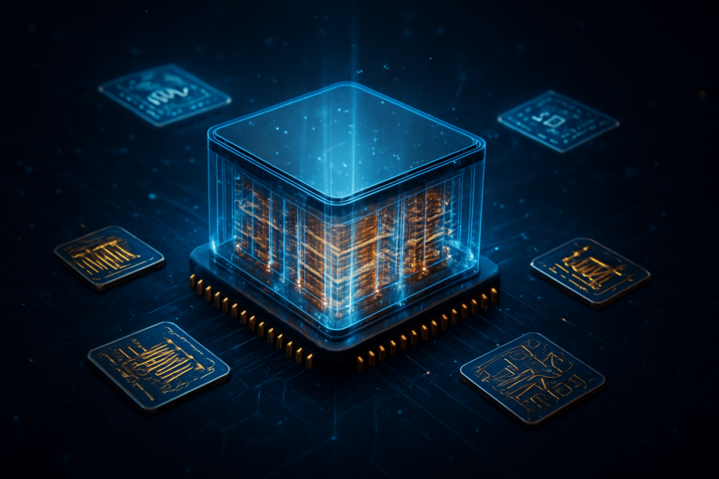
As of early 2026, the semiconductor landscape has reached a historic turning point, moving definitively away from the monolithic chip designs that defined the last fifty years. In their place, a new architecture known as 3.5D Advanced Packaging has emerged, powered by the Universal Chiplet Interconnect Express (UCIe) 3.0 standard. This development is not merely an incremental upgrade; it represents a fundamental shift in how artificial intelligence hardware is conceived, manufactured, and scaled, effectively turning the world’s most advanced silicon into a "plug-and-play" ecosystem.
The immediate significance of this transition is staggering. By moving away from "all-in-one" chips toward a modular "Silicon Lego" approach, the industry is overcoming the physical limits of traditional lithography. AI giants are no longer constrained by the maximum size of a single wafer exposure (the reticle limit). Instead, they are assembling massive "superchips" that combine specialized compute tiles, memory, and I/O from various sources into a single, high-performance package. This breakthrough is the engine behind the quadrillion-parameter AI models currently entering training cycles, providing the raw bandwidth and thermal efficiency necessary to sustain the next era of generative intelligence.
The 1,000x Leap: Hybrid Bonding and 3.5D Architectures
At the heart of this revolution is the commercialization of Copper-to-Copper (Cu-Cu) Hybrid Bonding. Traditional 2.5D packaging, which places chips side-by-side on a silicon interposer, relies on microbumps for connectivity. These bumps typically have a pitch of 40 to 50 micrometers. However, early 2026 has seen the mainstream adoption of Hybrid Bonding with pitches as low as 1 to 6 micrometers. Because interconnect density scales with the square of the pitch reduction, moving from a 50-micrometer bump to a 5-micrometer hybrid bond results in a 100x increase in area density. At the sub-micrometer level being pioneered for ultra-high-end accelerators, the industry is realizing a 1,000x increase in interconnect density compared to 2023 standards.
This 3.5D architecture combines the lateral scalability of 2.5D with the vertical density of 3D stacking. For instance, Broadcom (NASDAQ: AVGO) recently introduced its XDSiP (Extreme Dimension System in Package) architecture, which enables over 6,000 mm² of silicon in a single package. By stacking accelerator logic dies vertically before placing them on a horizontal interposer surrounded by 16 stacks of HBM4 memory, Broadcom has managed to reduce latency by up to 60% while cutting die-to-die power consumption by a factor of ten. This gapless connection eliminates the parasitic resistance of traditional solder, allowing for bandwidth densities exceeding 10 Tbps/mm.
The UCIe 3.0 specification, released in late 2025, serves as the "glue" for this hardware. Supporting data rates up to 64 GT/s—double that of the previous generation—UCIe 3.0 introduces a standardized Management Transport Protocol (MTP). This allows for "plug-and-play" interoperability, where an NPU tile from one vendor can be verified and initialized alongside an I/O tile from another. This standardization has been met with overwhelming support from the AI research community, as it allows for the rapid prototyping of specialized hardware configurations tailored to specific neural network architectures.
The Business of "Systems Foundries" and Chiplet Marketplaces
The move toward 3.5D packaging is radically altering the competitive strategies of the world’s largest tech companies. TSMC (NYSE: TSM) remains the dominant force, with its CoWoS-L and SoIC-X technologies being the primary choice for NVIDIA’s (NASDAQ: NVDA) new "Vera Rubin" architecture. However, Intel (NASDAQ: INTC) has successfully positioned itself as a "Systems Foundry" with its 18A-PT (Performance-Tuned) node and Foveros Direct 3D technology. By offering advanced packaging services to external customers like Apple (NASDAQ: AAPL) and Qualcomm (NASDAQ: QCOM), Intel is challenging the traditional foundry model, proving that packaging is now as strategically important as transistor fabrication.
This shift also benefits specialized component makers and EDA (Electronic Design Automation) firms. Companies like Synopsys (NASDAQ: SNPS) and Siemens (ETR: SIE) have released "Digital Twin" modeling tools that allow designers to simulate UCIe 3.0 links before physical fabrication. This is critical for mitigating the risk of "known good die" (KGD) failures, where one faulty chiplet could ruin an entire expensive 3.5D assembly. For startups, this ecosystem is a godsend; a small AI chip firm can now focus on designing a single, world-class NPU chiplet and rely on a standardized ecosystem to integrate it with industry-standard I/O and memory, rather than having to design a massive, risky monolithic chip from scratch.
Strategic advantages are also shifting toward those who control the memory supply chain. Samsung (KRX: 005930) is leveraging its unique position as both a memory manufacturer and a foundry to integrate HBM4 directly with custom logic dies using its X-Cube 3D technology. By moving logic dies to a 2nm process for tighter integration with memory stacks, Samsung is aiming to eliminate the "memory wall" that has long throttled AI performance. This vertical integration allows for a more cohesive design process, potentially offering higher yields and lower costs for high-volume AI accelerators.
Beyond Moore’s Law: A New Era of AI Scalability
The wider significance of 3.5D packaging and UCIe cannot be overstated; it represents the "End of the Monolithic Era." For decades, the industry followed Moore’s Law by shrinking transistors. While that continues, the primary driver of performance has shifted to interconnect architecture. By disaggregating a massive 800mm² GPU into eight smaller 100mm² chiplets, manufacturers can significantly increase wafer yields. A single defect that would have ruined a massive "superchip" now only ruins one small tile, drastically reducing waste and cost.
Furthermore, this modularity allows for "node mixing." High-performance logic can be restricted to the most expensive 2nm or 1.4nm nodes, while less sensitive components like I/O and memory controllers can be "back-ported" to cheaper, more mature 6nm or 5nm nodes. This optimizes the total cost per transistor and ensures that leading-edge fab capacity is reserved for the most critical components. This pragmatic approach to scaling mirrors the evolution of software from monolithic applications to microservices, suggesting a permanent change in how we think about compute hardware.
However, the rise of the chiplet ecosystem does bring concerns, particularly regarding thermal management. Stacking high-power logic dies vertically creates intense heat pockets that traditional air cooling cannot handle. This has sparked a secondary boom in liquid-cooling technologies and "rack-scale" integration, where the chip, the package, and the cooling system are designed as a single unit. As AMD (NASDAQ: AMD) prepares its Instinct MI400 for release later in 2026, the focus is as much on the liquid-cooled "CDNA 5" architecture as it is on the raw teraflops of the silicon.
The Future: HBM5, 1.4nm, and the Chiplet Marketplace
Looking ahead, the industry is already eyeing the transition to HBM5 and the integration of 1.4nm process nodes into 3.5D stacks. We expect to see the emergence of a true "chiplet marketplace" by 2027, where hardware designers can browse a catalog of verified UCIe-compliant dies for various functions—cryptography, video encoding, or specific AI kernels—and have them assembled into a custom ASIC in a fraction of the time it takes today. This will likely lead to a surge in "domain-specific" AI hardware, where chips are optimized for specific tasks like real-time translation or autonomous vehicle edge-processing.
The long-term challenges remain significant. Standardizing test and assembly processes across different foundries will require unprecedented cooperation between rivals. Furthermore, the complexity of 3.5D power delivery—getting electricity into the middle of a stack of chips—remains a major engineering hurdle. Experts predict that the next few years will see the rise of "backside power delivery" (BSPD) as a standard feature in 3.5D designs to address these power and thermal constraints.
A Fundamental Paradigm Shift
The convergence of 3.5D packaging, Hybrid Bonding, and the UCIe 3.0 standard marks the beginning of a new epoch in computing. We have moved from the era of "scaling down" to the era of "scaling out" within the package. This development is as significant to AI history as the transition from CPUs to GPUs was a decade ago. It provides the physical infrastructure necessary to support the transition from generative AI to "Agentic AI" and beyond, where models require near-instantaneous access to massive datasets.
In the coming weeks and months, the industry will be watching the first production yields of NVIDIA’s Rubin and AMD’s MI400. These products will serve as the litmus test for the viability of 3.5D packaging at massive scale. If successful, the "Silicon Lego" model will become the default blueprint for all high-performance computing, ensuring that the limits of AI are defined not by the size of a single piece of silicon, but by the creativity of the architects who assemble them.
This content is intended for informational purposes only and represents analysis of current AI developments.
TokenRing AI delivers enterprise-grade solutions for multi-agent AI workflow orchestration, AI-powered development tools, and seamless remote collaboration platforms.
For more information, visit https://www.tokenring.ai/.